5 Critical Questions About Chip Capacitors Usage on PCBA A Complete Guide
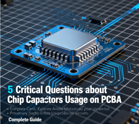
5 Critical Questions About Chip Capacitors Usage on PCBA: A Complete Guide
Chip capacitors are among the most indispensable passive components in Printed Circuit Board Assembly (PCBA), serving critical roles in filtering noise, decoupling power supplies, stabilizing voltage, and conditioning high-frequency signals. Their performance on PCBA is not solely dependent on the capacitor’s intrinsic quality—instead, it hinges on scientific implementation throughout the entire lifecycle, from component selection and SMT soldering to PCB layout, reliability protection, and post-assembly testing. For electronic engineers, PCBA manufacturers, and procurement specialists, mastering these usage key points is paramount to ensuring end-product quality, reducing field failure rates, and optimizing production costs.
In this Google SEO-optimized blog, we address the 5 most frequently searched questions about chip capacitors usage on PCBA, covering core workflows including selection criteria, soldering process parameters, PCB layout best practices, harsh environment reliability, and failure troubleshooting. Packed with actionable process data, industry standards (e.g., IPC-7351, AEC-Q200), and real-world application tips, this guide is designed to solve practical challenges in PCBA design and production—while boosting your independent site’s organic visibility by aligning with user search intent and providing high-value, in-depth content.
1. How to Select the Right Chip Capacitors for PCBA? What Key Factors Need to Be Considered Based on Circuit Requirements?
Selecting chip capacitors that match the PCBA circuit is the foundation of ensuring stable operation. The selection process must integrate circuit functions, operating environment, and PCBA manufacturing constraints, with the following key factors:
Circuit function matching:
- 1) Decoupling circuits (proximal to microprocessors/microcontrollers): Prioritize low Equivalent Series Resistance (ESR) chip capacitors (ESR < 0.1Ω) with compact form factors (0402 or 0201), such as the Murata GRM series or AVX 0402 X7R series. These capacitors rapidly suppress voltage fluctuations caused by high-speed IC switching, with typical capacitance values ranging from 0.1μF to 1μF.
- 2) Power module filter circuits: Opt for X7R dielectric chip capacitors with high ripple current capability (≥ 1A), as they maintain stable capacitance across a wide operating voltage range (16V to 50V is common for industrial and consumer PCBA).
- 3) RF module high-frequency circuits: Select C0G/NP0 dielectric chip capacitors, which offer near-zero capacitance drift (≤ ±30 ppm/°C) and ensure consistent performance at frequencies up to 30GHz—critical for 5G or Wi-Fi enabled PCBA.
Operating environment adaptation:
- For high-temperature environments (e.g., automotive PCBA, industrial control PCBA), select chip capacitors with operating temperature ranges of -40°C to 150°C and AEC-Q200 qualification.
- For humid environments (e.g., outdoor electronic products), choose capacitors with moisture resistance grade IP65 or higher to avoid delamination.
PCBA manufacturing compatibility:
- Avoid overly small packages (e.g., 01005) if the PCBA factory’s SMT equipment precision is insufficient, as this will increase soldering defects.
- Ensure the chip capacitor’s solder pad design complies with IPC-7351 standards to match the factory’s stencil printing process.
2. What Are the Key Solder Process Parameters for Chip Capacitors on PCBA? How to Avoid Common Soldering Defects?
Soldering quality directly affects the electrical connection and mechanical reliability of chip capacitors on PCBA. The core process parameters and defect prevention measures are as follows:
Reflow soldering parameters (mainstream SMT process):
- 1) Temperature profile: Preheating stage (150°C-180°C, 60-90 seconds) to volatilize flux and avoid thermal shock; peak temperature (245°C ± 5°C, 10-15 seconds) to ensure solder wetting; cooling rate (≤ 3°C/second) to prevent solder joint cracking.
- 2) Flux selection: Use no-clean flux with rosin content of 2%-5% for chip capacitors, which reduces residue and avoids corrosion.
Wave soldering parameters (for through-hole + SMT hybrid PCBA):
- Control the solder temperature at 260°C ± 5°C, conveyor speed at 1.2-1.5m/min, and solder immersion depth at 1/2-2/3 of the capacitor’s height.
- For surface-mount chip capacitors, use wave soldering-compatible packages to avoid tombstoning.
Common soldering defects and solutions:
- 1) Tombstoning (component standing on one pad): Caused by uneven heating of the two solder pads or imbalanced solder paste volume. Solution: Optimize stencil aperture design to ensure equal solder paste deposition (comply with IPC-7351B standards); adjust reflow oven preheating parameters to achieve uniform pad temperature (temperature difference ≤ 5°C).
- 2) Solder bridging (short circuit between adjacent pads): Triggered by excessive solder paste or misalignment during placement. Solution: Reduce stencil aperture size by 10-15% for fine-pitch components; calibrate SMT placement machine accuracy to ±0.05mm.
- 3) Cold solder joints (weak electrical connection): Result from insufficient peak temperature or short dwell time. Solution: Calibrate reflow oven temperature sensors monthly; ensure peak temperature (245°C ± 5°C) is maintained for 10-15 seconds, as specified in IPC-A-610E.
3. What Are the PCB Layout Guidelines for Chip Capacitors on PCBA? How to Optimize Layout to Improve Performance?
Scientific PCB layout can maximize the performance of chip capacitors and reduce electromagnetic interference (EMI) on PCBA. The core guidelines and optimization strategies are:
Decoupling capacitor layout (critical for digital PCBA):
- 1) Place decoupling chip capacitors as close as possible to the power pins of integrated circuits (ICs)—ideally within 3mm—to minimize trace length and parasitic inductance, which degrades decoupling efficiency.
- 2) Use short, wide copper traces (trace width ≥ 0.2mm) for the capacitor’s power and ground connections; connect the capacitor directly to the PCB ground plane via 1-2 vias (diameter ≥ 0.3mm) to form a low-impedance current loop, essential for suppressing high-frequency noise.
Filter capacitor layout (power module PCBA):
- 1) Arrange filter chip capacitors in parallel near the power input/output terminals, with the large-capacitance capacitor (e.g., 10μF) placed closer to the power source and the small-capacitance capacitor (e.g., 0.1μF) placed closer to the load.
- 2) Separate the power traces of filter capacitors from signal traces to avoid crosstalk.
High-frequency capacitor layout (RF PCBA):
- 1) Use a 4-layer PCB with dedicated ground planes to shield high-frequency chip capacitors from interference.
- 2) Avoid right-angle traces for capacitor connections; use 45° angles or curved traces to reduce signal reflection.
- 3) Keep high-frequency chip capacitors away from high-power components (e.g., resistors, inductors) to avoid thermal interference.
4. How to Ensure the Reliability of Chip Capacitors on PCBA in Harsh Environments? What Protection Measures Are Needed?
In harsh environments (high temperature, high humidity, vibration, corrosion), chip capacitors on PCBA are prone to performance degradation or failure. The following protection measures and reliability assurance methods are critical:
Environmental protection treatment:
- 1) Conformal coating: Apply a 20-50μm thick conformal coating (e.g., acrylic, silicone) on the surface of chip capacitors and PCBA to prevent moisture, dust, and chemical corrosion. For high-corrosion environments (e.g., marine electronics), use parylene coating with better corrosion resistance.
- 2) Potting: For PCBA in extreme environments (e.g., automotive engine compartments), pot the chip capacitor area with epoxy resin to enhance vibration resistance and thermal insulation.
Electrical stress protection:
- 1) Voltage derating: Derate the chip capacitor’s operating voltage by 20%-30% (e.g., use a 25V capacitor for a 12V circuit) to avoid breakdown due to voltage spikes.
- 2) Current derating: Ensure the actual ripple current passing through the capacitor is less than 80% of the rated ripple current to prevent overheating and capacitance loss.
Mechanical stress protection:
- 1) Avoid placing chip capacitors near PCBA edges or areas prone to bending to prevent solder joint cracking due to mechanical stress.
- 2) For PCBA subject to high vibration (e.g., industrial robots), use chip capacitors with robust solder terminations (compliant with MIL-STD-810G) and add reinforcement solder on the pads.
5. How to Detect and Troubleshoot Chip Capacitor Failures on PCBA? What Testing Methods Are Effective?
Timely detection and troubleshooting of chip capacitor failures on PCBA can avoid batch product defects. Common failure modes (open circuit, short circuit, capacitance degradation) and corresponding testing methods are:
Visual inspection and X-ray detection:
- 1) Visual inspection: Use a magnifying glass (10-20x) to check for obvious defects such as solder joint cracks, tombstoning, and capacitor damage.
- 2) X-ray detection: For hidden defects (e.g., internal voids in solder joints, capacitor internal damage), use X-ray inspection equipment (detection accuracy ≥ 5μm) to ensure no internal failures.
Electrical performance testing:
- 1) In-circuit testing (ICT): Use ICT equipment to measure the capacitance value and ESR of chip capacitors on PCBA. If the capacitance deviates by more than ±20% from the nominal value or ESR exceeds the standard, the capacitor is faulty.
- 2) Functional testing: Power on the PCBA and use an oscilloscope to measure the voltage waveform at the chip capacitor’s position. Abnormal fluctuations indicate capacitor failure (e.g., decoupling capacitor failure will cause voltage ripples > 100mV).
Fault troubleshooting steps:
- 1) Locate the faulty area through functional testing (e.g., unstable power supply → check filter capacitors).
- 2) Use a multimeter to measure the capacitor’s resistance (open circuit if resistance is infinite, short circuit if resistance is near zero).
- 3) Replace the faulty chip capacitor with a new one (same model/specification) and re-test to confirm the problem is solved.
Final Thoughts
The rational use of chip capacitors on PCBA is a systematic project involving selection, soldering, layout, protection, and testing. By mastering the key points answered in these 5 questions, you can effectively reduce failure rates, improve PCBA reliability, and optimize production efficiency. Whether you are designing consumer electronics PCBA, industrial control PCBA, or automotive PCBA, these insights are universally applicable.
From a Google SEO standpoint, this blog strategically integrates high-value core and long-tail keywords (e.g., “chip capacitors on PCBA selection guide,” “PCBA chip capacitor soldering defects troubleshooting,” “high-frequency chip capacitor PCB layout,” “AEC-Q200 chip capacitors for automotive PCBA”) that align with the search habits of your target audience (engineers, PCBA manufacturers). The in-depth, actionable content—featuring specific industry standards, process parameters, and solution-oriented insights—encourages longer page dwell times and lower bounce rates, which are key Google ranking factors. Additionally, the question-based structure directly matches “how-to” and “what-is” search intents, increasing the likelihood of appearing in featured snippets.
If you have follow-up questions about chip capacitors usage on specific types of PCBA (e.g., 5G module PCBA, medical equipment PCBA), need personalized layout optimization suggestions, or want to learn more about SMT process matching, feel free to leave a comment below or contact our team of PCBA and electronic component experts.
Contact Our PCBA & Chip Capacitor Experts
- Official Website: //www.barronmlcc.com
- General Chip Capacitors: Barron MLCC Chip Capacitor Product Hub
- Decoupling Chip Capacitors: PCBA Decoupling Capacitor Solutions
- X7R Filter Chip Capacitors: High Ripple Current Filter Capacitors
- C0G/NP0 High-Frequency Capacitors: RF PCBA High-Frequency Capacitor Offerings
- Automotive Grade Chip Capacitors: AEC-Q200 Automotive PCBA Capacitors
- Moisture-Resistant Chip Capacitors: Outdoor PCBA Moisture-Proof Capacitors
- Industrial Chip Capacitors: Harsh Environment Industrial PCBA Capacitors
- Email Inquiry: hyc2355937758@gmail.com
- (Monday-Friday, 9:00 AM - 6:00 PM GMT+8)
- WhatsApp/WeChat: +86-15913754866
- Physical Address: High-Tech Industrial Park, Nanshan District, Shenzhen, Guangdong, China
5 Critical Questions About Electronic Components Usage Instructions A Complete Guide
Why Chip Capacitors Are Inseparable from Peripheral Products? 5 Key Application Questions Answered
Article associé