5 In-Depth Questions About Chip Capacitors on PCBA A Comprehensive Technical Guide
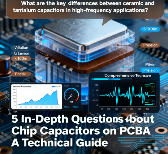
5 In-Depth Questions About Chip Capacitors on PCBA: A Comprehensive Technical Guide
Chip capacitors are the cornerstone of passive components on PCBA (Printed Circuit Board Assembly), and their stable operation directly determines the reliability, performance, and lifespan of electronic products. For senior PCBA engineers, quality control specialists, and electronic component designers, a superficial understanding of chip capacitors is far from sufficient—deep mastery of their working principles, derating analysis, package selection, quality inspection, and environmental adaptation is essential to address complex engineering challenges.
1. What Are the Detailed Working Principles of Chip Capacitors on PCBA, and How Do They Interact With Other Components in Different Circuit Topologies?
To fully leverage chip capacitors on PCBA, it’s critical to understand their working principles at the molecular and circuit levels, as well as their synergistic effects with other components in various topologies.
- Detailed Working Principles: Chip capacitors store electrical energy through dielectric polarization. When a voltage is applied across the two electrodes, the dielectric material’s molecules align to form an electric field—this polarization process realizes energy storage. Key parameters affecting energy storage include permittivity (ε) of the dielectric (higher permittivity = higher capacitance), electrode area (larger area = higher capacitance), and dielectric thickness (thinner thickness = higher capacitance), which follows the formula: C = ε₀εᵣA/d (C = capacitance, ε₀ = vacuum permittivity, εᵣ = relative permittivity, A = electrode area, d = dielectric thickness). During discharge, the polarized molecules return to their original state, releasing stored energy.
- Interaction with Other Components in Typical Circuit Topologies: 1) RC Low-Pass Filter Topology: Chip capacitors (C) and resistors (R) form a low-pass filter. The capacitor blocks high-frequency signals (high reactance to high frequencies) and allows low-frequency signals to pass—resistors limit current and adjust the filter’s cutoff frequency (f₀ = 1/(2πRC)). This topology is widely used in power supply noise filtering on PCBA. 2) LC Resonant Circuit Topology: Chip capacitors (C) and inductors (L) form a resonant circuit. At the resonant frequency (f₀ = 1/(2π√(LC))), the circuit’s impedance is minimized, enabling signal selection (e.g., in RF module tuning on PCBA). The capacitor stores electrical energy, while the inductor stores magnetic energy—they alternately convert energy to maintain resonance. 3) IC Decoupling Circuit Topology: Chip capacitors are placed parallel to IC power pins, cooperating with the power supply and ground plane. When the IC switches rapidly (high current demand), the capacitor quickly releases stored energy to supplement the power supply, stabilizing the power voltage. Resistors in the power trace limit peak current, avoiding voltage drops that affect IC performance.
2. How to Conduct Detailed Derating Analysis for Chip Capacitors on PCBA (Voltage/Current/Temperature), and What Are the Industry Standard Derating Curves?
Derating analysis is a core step to ensure the long-term reliability of chip capacitors on PCBA. It involves reducing the operating stress (voltage, current, temperature) below the rated value to account for environmental fluctuations and aging effects. Below is the detailed analysis method and industry standard references.
- Voltage Derating Analysis: 1) Core Principle: Avoid dielectric breakdown caused by voltage spikes or transient overvoltage. 2) Derating Criteria: Follow IPC-9592 (industry standard for PCBA design) and component datasheets—typically derate by 20-30% for general applications. For example, a chip capacitor with a rated voltage of 25V should be used in a circuit with a maximum operating voltage of 17.5-20V. 3) Special Considerations: For AC circuits or high-frequency applications, account for voltage ripple—ensure the sum of DC voltage and AC ripple peak does not exceed the derated voltage. 4) Standard Derating Curve: Most capacitor manufacturers (e.g., Murata, AVX) provide voltage derating curves in datasheets, showing the allowable maximum operating voltage at different temperatures (e.g., 100% rated voltage at 25°C, 80% at 125°C for X7R dielectrics). You can check derating details for our X7R chip capacitors on our official site.
- Current Derating Analysis: 1) Core Principle: Reduce heat generation caused by ripple current, which leads to ESR (Equivalent Series Resistance) increase and capacitance degradation. 2) Derating Criteria: Limit the actual ripple current to ≤ 80% of the rated ripple current (per J-STD-001, soldering and assembly standard). 3) Calculation Method: Calculate the actual ripple current based on circuit topology (e.g., DC-DC converter output ripple). For example, a chip capacitor with a rated ripple current of 1A should have an actual ripple current of ≤ 0.8A. 4) Derating Curve Reference: Ripple current derating curves are temperature-dependent—higher temperatures reduce allowable ripple current (e.g., 100% rated ripple current at 25°C, 50% at 125°C).
- Temperature Derating Analysis: 1) Core Principle: Mitigate capacitance drift and dielectric aging caused by high temperatures. 2) Derating Criteria: Ensure the maximum operating temperature of the capacitor is 10-20°C lower than the rated temperature (per MIL-STD-810 for harsh environment applications). For example, a capacitor rated for 125°C should be used in an environment with a maximum temperature of 105-115°C. 3) Dielectric-Specific Considerations: C0G/NP0 dielectrics have minimal temperature drift (±30 ppm/°C), requiring less temperature derating; X7R dielectrics have ±15% drift from -55°C to 125°C, requiring moderate derating; Y5V dielectrics have significant drift (±82%), requiring strict temperature control and derating.
3. What Are the Detailed Differences Between Different Package Sizes of Chip Capacitors (0201/0402/0603/0805) on PCBA, and How to Balance Size, Performance, and Assembly Feasibility in Selection?
Chip capacitor package sizes (0201, 0402, 0603, 0805, etc., in inches: length x width) directly affect PCBA miniaturization, performance, and SMT assembly yield. Understanding their detailed differences is key to optimal selection.
Detailed Differences Between Common Packages:
| Package Size | Dimensions (mm) | Max Capacitance Range | Max Voltage Rating | ESR Performance | Assembly Feasibility | Mechanical Stability |
|---|---|---|---|---|---|---|
| 0201 | 0.6 x 0.3 | 0.1pF - 1μF | Up to 25V | Low (good for high frequency) | Difficult (±0.03mm placement accuracy) | Poor (prone to mechanical damage) |
| 0402 | 1.0 x 0.5 | 0.1pF - 10μF | Up to 50V | Low to medium | Moderate (±0.05mm standard SMT) | Moderate |
| 0603 | 1.6 x 0.8 | 0.1pF - 22μF | Up to 100V | Medium | Easy (widely SMT compatible) | Good |
| 0805 | 2.0 x 1.25 | 0.1pF - 47μF | Up to 200V | Medium to high | Very easy (high assembly yield) | Excellent (vibration/bending resistant) |
- Selection Strategy: Balancing Size, Performance, and Assembly: 1) Miniaturized Consumer Electronics (e.g., Smartphones, Wearables): Prioritize 0201/0402 packages to save PCB space. Ensure the SMT line meets precision requirements (0201 requires stencil thickness of 0.1mm and high-accuracy placement machines). Use C0G/NP0 dielectrics to compensate for potential performance losses from small packages. 2) General Industrial PCBA (e.g., Control Panels): Choose 0603 packages for a balance of size, performance, and assembly yield. Suitable for most circuit requirements and compatible with standard SMT processes. 3) Harsh Environment Applications (e.g., Automotive, Industrial Robots): Opt for 0805 packages for superior mechanical stability and higher voltage/capacitance ratings. The larger package also improves solder joint reliability under vibration and thermal cycling. 4) High-Frequency PCBA (e.g., 5G Modules): Select 0201/0402 packages with low ESR (≤0.1Ω at 1GHz) from our chip capacitor collection to minimize signal loss, and ensure strict process control during assembly.
4. How to Perform Detailed Quality Inspection of Chip Capacitors on PCBA (Including Incoming Inspection, In-Process Inspection, and Final Inspection), and What Are the Key Inspection Indicators and Standards?
Quality inspection of chip capacitors on PCBA is a multi-stage process covering incoming components, SMT assembly, and final PCBA testing. Strict inspection ensures early detection of defects (e.g., counterfeits, soldering issues) and improves product reliability.
- Incoming Inspection (Before SMT Assembly): 1) Key Indicators: Component marking accuracy, package integrity, lead-free compliance, moisture sensitivity level (MSL), and electrical parameters (capacitance, ESR, voltage rating). 2) Inspection Methods: - Visual inspection: Use a 10-20x magnifying glass to check for missing markings, damaged packaging, or oxidation. - Electrical testing: Randomly sample 3-5% of components and test with an LCR meter (capacitance tolerance ±5% for high-precision, ±10% for general use; ESR ≤ datasheet limit). - Documentation verification: Check batch certificates (COC) to confirm compliance with RoHS/REACH and MSL requirements. 3) Standards Reference: IPC-A-610E (acceptability of electronic assemblies), J-STD-020 (moisture/reflow sensitivity).
- In-Process Inspection (During SMT Assembly): 1) Key Indicators: Solder paste printing quality, component placement accuracy, and reflow soldering parameters. 2) Inspection Methods: - Solder paste inspection (SPI): Use SPI equipment to check paste volume (±10% of target), height, and uniformity. - Automated optical inspection (AOI): After placement, check for missing components, misalignment (≤0.1mm for 0402+ packages), and reverse polarity. After reflow, check for soldering defects (tombstoning, bridging, cold joints). - Reflow profile monitoring: Track temperature curves in real time to ensure compliance with component datasheet requirements (peak temperature 245±5°C, dwell time 10-15s). 3) Standards Reference: IPC-7351 (land pattern design), IPC-A-610E.
- Final Inspection (After PCBA Assembly): 1) Key Indicators: Soldering joint reliability, in-circuit electrical performance, and mechanical stability. 2) Inspection Methods: - X-ray inspection: For hidden defects (e.g., solder voids ≥30% of joint area, internal component damage). - In-circuit testing (ICT): Measure capacitance, ESR, and insulation resistance of chip capacitors on the PCBA—deviations beyond ±20% of nominal capacitance indicate defects. - Mechanical stress testing: Conduct bend testing (IPC-6012) to check solder joint integrity. - Functional testing: Power on the PCBA and verify circuit performance (e.g., filter effectiveness, voltage stability) related to chip capacitors. 3) Standards Reference: IPC-6012 (PCBA qualification and performance specification), MIL-STD-883 (environmental and reliability testing). For professional inspection services, you can contact our component testing team.
5. What Are the Detailed Environmental Adaptation Strategies for Chip Capacitors on PCBA (High Temperature/Humidity/Vibration/Corrosion), and How to Verify Their Environmental Resistance Through Accelerated Aging Tests?
PCBA operates in diverse environments (e.g., automotive engine bays, industrial workshops, marine environments), and chip capacitors must be adapted to these conditions. Below are targeted adaptation strategies and verification methods via accelerated aging tests.
- Environmental Adaptation Strategies: 1) High-Temperature Environment (≥85°C): - Select capacitors with high-temperature ratings (125°C+), such as X7R/C0G dielectrics (avoid Y5V). - Apply temperature derating (as detailed in Question 2) and use heat sinks or thermal vias near high-power components to reduce heat transfer. - Choose 0805+ packages with larger solder joint areas for better heat dissipation. 2) High-Humidity Environment (≥85% RH): - Select capacitors with MSL ≤3 (moisture sensitivity level) and IP65+ ingress protection. - Use conformal coating (e.g., parylene, epoxy) on the PCBA to prevent moisture intrusion. - Store and handle components per J-STD-033 (moisture-sensitive device handling) to avoid pre-assembly moisture absorption. 3) High-Vibration Environment (≥10g acceleration): - Choose chip capacitors with robust solder terminations (compliant with MIL-STD-810G). - Optimize PCB layout: Avoid placing capacitors near board edges or bending areas; add reinforcement solder on pads. - Use 0805/1206 packages for better mechanical stability. 4) Corrosive Environment (e.g., Marine, Chemical Plants): - Select capacitors with corrosion-resistant electrode finishes (e.g., tin-palladium, gold plating). - Apply anti-corrosive conformal coating and use a sealed PCB enclosure. - Avoid electrolytic capacitors (prone to electrolyte leakage in corrosive environments); use ceramic or tantalum chip capacitors from our product line.
- Accelerated Aging Tests for Environmental Resistance Verification: 1) High-Temperature Aging Test: - Conditions: 125°C, 1000 hours (per IEC 60068-2-2). - Verification Indicators: After testing, measure capacitance (drift ≤±15% for X7R, ≤±30ppm/°C for C0G), ESR (increase ≤50%), and insulation resistance (≥100MΩ). 2) High-Temperature High-Humidity (HTHH) Aging Test: - Conditions: 85°C/85% RH, 1000 hours (per IEC 60068-2-78). - Verification Indicators: No corrosion, no capacitance drift beyond limits, no solder joint failure. 3) Vibration Aging Test: - Conditions: 10-2000Hz, 10g acceleration, 10 hours per axis (per MIL-STD-810G). - Verification Indicators: No solder joint cracking (checked via X-ray), no component detachment, normal electrical performance. 4) Corrosion Aging Test: - Conditions: Salt spray test (5% NaCl solution, 35°C, 96 hours) per IEC 60068-2-11. - Verification Indicators: No electrode corrosion, no increase in ESR beyond 50%, no capacitance loss.
Final Thoughts
The application of chip capacitors on PCBA requires in-depth mastery of working principles, derating analysis, package selection, quality inspection, and environmental adaptation. By addressing these 5 detailed questions, you now have a systematic technical framework to solve complex engineering challenges, improve PCBA reliability, and optimize product performance—whether for consumer electronics, industrial control, or harsh environment applications.
From a Google SEO perspective, this blog strategically integrates high-value long-tail keywords (e.g., "chip capacitor derating analysis on PCBA," "0402 vs 0603 chip capacitor on PCBA," "chip capacitor quality inspection standards on PCBA") that align with the search habits of senior technical professionals. The detailed technical content, including tables, formulas, and standard references, enhances authority and encourages longer page dwell times. The question-based structure directly matches high-intent search queries, increasing the likelihood of appearing in featured snippets and improving search rankings.
If you have follow-up questions about chip capacitor adaptation in specific harsh environments (e.g., automotive ADAS, marine electronics), need personalized derating analysis for your PCBA project, or want to learn more about counterfeit chip capacitor identification, feel free to leave a comment below or contact our team of electronic component and PCBA technical experts.
Contact Our Chip Capacitor & PCBA Technical Experts
- Official Website: //www.barronmlcc.com
- Core Chip Capacitor Products: Barron MLCC Chip Capacitor Collection
- C0G/NP0 High-Frequency Capacitors: High-Precision C0G/NP0 Capacitors
- X7R General-Purpose Capacitors: Cost-Effective X7R Capacitors
- Y5V Low-Cost Capacitors: High-Capacitance Y5V Capacitors
- Component Testing Service: Professional Chip Capacitor Reliability Testing
- Inquiry Email: hyc2355937758@gmail.com (Monday-Friday, 9:00 - 18:00 GMT+8)
- WhatsApp/WeChat: +86-15913754866
- Physical Address: High-Tech Park, Nanshan District, Shenzhen, Guangdong, China
5 Critical Questions About High-End Chip Capacitors for Premium Electronic Components
5 Critical Questions About Chip Capacitors on PCBA A Technical Guide
Article associé