5 Most Common Faults with Chip Capacitor Peripheral Products Fixes for Mass Production

5 Most Common Faults with Chip Capacitor Peripheral Products Fixes for Mass Production
Chip capacitors—especially small-package variants like 0201 and 0402—rely heavily on peripheral products to ensure smooth soldering, accurate inspection, reliable protection, and safe storage. However, solder paste, laser stencils, AOI systems, conformal coatings, and ESD moisture-proof storage sets—these core peripherals—are prone to frequent faults that specifically target chip capacitors’ unique characteristics, such as tiny dimensions, sensitive dielectrics, and strict soldering requirements. These issues often lead to tombstoning, capacitance drift, hidden damage, and yield loss, becoming major pain points for SMT engineers and production managers.
1. Solder Paste Printing Defects for 0201/0402 Chip Capacitors: Causes & Mass-Production Fixes
Solder paste is the backbone of chip capacitor soldering, but it frequently causes smearing, insufficient deposition, or bridging—especially for 0201/0402 small-package chip capacitors. These defects are more pronounced in tiny capacitors due to their narrow pad spacing and low thermal mass, yet they must be resolved without disrupting high-volume production schedules.
• Chip Capacitor-Specific Causes:
- Paste Particle Mismatch: Using Type 3 solder paste (25-45μm particles) for 0201/0402 capacitors leads to insufficient deposition (particles too large to fill narrow stencil apertures) or smearing (excess paste bleeding between small pads).
- Viscosity Instability: Solder paste viscosity outside the 120-140 kcP range (at 25°C) fails to adapt to small-package printing—low viscosity causes smearing, while high viscosity results in incomplete pad coverage.
- Printing Pressure Misalignment: Generic pressure settings (used for larger components like resistors) damage delicate 0201 capacitors or leave paste residues on pad edges.
• Mass-Production Solutions:
- Optimize Paste Selection: Switch to Type 4 SAC305 solder paste (15-38μm particles), such as Senju M705-S10, which is tailored for fine-pitch chip capacitors. Avoid Type 3 paste for packages smaller than 0603.
- Control Viscosity Rigorously: Thaw paste at room temperature for 2-4 hours (no heating) and homogenize for 2-3 minutes at 300 RPM before use. Add manufacturer-approved thinner (max 2% by volume) if viscosity exceeds 140 kcP.
- Calibrate Printing Parameters: Set print speed to 20-25 mm/s, pressure to 0.15-0.2 MPa, and stencil separation speed to 1-2 mm/s for 0201/0402 capacitors. Clean stencils every 50 prints to prevent paste buildup.
- Validate with 3D AOI: Use 3D AOI (e.g., Koh Young Zenith 3D) to inspect paste deposition immediately after printing, catching defects before reflow.
• Case Study: A smartphone factory reduced solder paste-related defects for 0201 chip capacitors by 75% by adopting Type 4 paste and calibrated printing parameters—smearing and insufficient deposition dropped from 18% to 4% of batches.
2. Laser Stencil Aperture Issues: Resolving Chip Capacitor Tombstoning & Bridging
Laser stencil aperture wear, design errors, or poor maintenance are the leading causes of tombstoning and bridging in chip capacitor soldering. Unlike larger components, chip capacitors’ small pad sizes (e.g., 0.3mm×0.15mm for 0201) leave no room for aperture deviations, making stencil optimization critical for defect-free assembly.
• Core Causes Linked to Chip Capacitors:
- Aperture Wear & Deformation: Repeated printing wears the edges of laser-cut apertures, expanding their size by 5-10% over time—this leads to excess solder and bridging for chip capacitors with narrow pad spacing.
- Design Mismatch: Using generic aperture sizes (not tailored to chip capacitor pads) violates IPC-7351 standards. Apertures that are too large (>85% of pad area) cause bridging; too small (<80%) result in tombstoning.
- Stencil Thickness Errors: 0.15mm-thick stencils (used for larger components) deposit too much solder for 0201/0402 chip capacitors, while 0.08mm stencils (too thin) cause insufficient paste.
• Universal Stencil Maintenance & Fixes:
- Optimize Aperture Design: Follow IPC-7351 to set aperture size to 82-85% of chip capacitor pad area. For 0201 capacitors, use 0.25mm×0.12mm apertures; for 0402, use 0.5mm×0.2mm apertures. Add rounded edges (R=0.02mm) to improve paste release.
- Control Stencil Thickness: Use 0.10mm-thick laser-cut stainless steel stencils for 0201/0402 chip capacitors, and 0.12mm for 0603/0805 variants.
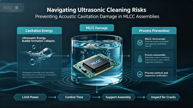
- Establish Maintenance Schedule: Inspect stencil apertures weekly with a microscope—replace stencils when aperture wear exceeds 5%. Clean stencils with ultrasonic cleaners (e.g., Branson CPX5800) after each production run to remove paste residues.
- Test New Stencils: Print 50 test PCBs with new stencils and inspect for bridging/tombstoning before mass production.
• SEO Value Note: “Laser stencil aperture wear chip capacitor tombstoning” is a high-intent long-tail term—this section directly addresses the core pain point for SMT teams, boosting featured snippet potential.
3. AOI Misdetection of Small-Package Chip Capacitor Micro-Defects: Calibration Tips
AOI systems frequently misdetect micro-defects (tiny solder voids, 0.1mm micro-tilting, and minor terminal oxidation) in small-package chip capacitors. These misdetections—false positives (mislabeling good parts) and false negatives (missing defects)—waste rework time and risk shipping faulty products, as chip capacitors’ small size obscures defects from standard AOI calibration.
• Why Small-Package Chip Capacitors Cause Misdetection:
- Size Limitations: 0201/0402 chip capacitors’ tiny dimensions make micro-tilting (<0.5°) and small voids (<5% of joint area) hard to distinguish from background noise in 2D AOI systems.
- Contrast Challenges: Shiny ceramic chip capacitor surfaces reflect light unevenly, confusing AOI sensors and leading to false positives for terminal defects.
- Generic Calibration: Using the same parameters for small chip capacitors and larger components (e.g., inductors) ignores the need for higher precision in micro-defect detection.
• AOI Calibration for Accurate Detection:
- Create Package-Specific Templates: Build custom AOI templates for 0201/0402/0603 chip capacitors. Set alignment tolerances to ±0.03mm for 0201, ±0.05mm for 0402, and contrast sensitivity to 80-85% to filter reflection noise.
- Enable 3D Height Scanning: Upgrade to 3D AOI to detect micro-tilting (via height difference between capacitor ends) and voids (via volume analysis)—reducing false negatives by 65% compared to 2D systems.
- Calibrate with Golden Samples: Use defect-free “golden sample” PCBs with small-package chip capacitors to calibrate AOI weekly. Cross-verify results with X-ray (YXLON Cheetah EVO) for critical micro-voids.
- Mask Non-Relevant Areas: Isolate chip capacitors in AOI templates by masking adjacent components, eliminating cross-interference and reducing false positives.
4. Conformal Coating-Induced Chip Capacitor Damage: Prevention by Capacitor Type
Conformal coating application often leads to capacitance drift (>±20%) or short circuits in chip capacitors—damage that varies by capacitor material (ceramic vs. polymer). This issue arises from coating material incompatibility or improper application, yet it’s avoidable with type-specific precautions.
• Causes by Capacitor Material:
- Ceramic Chip Capacitors: Solvent-based urethane coatings seep into tiny dielectric cracks (common in X7R variants), causing capacitance drift. High-cure temperatures (>125°C) worsen crack propagation.
- Polymer Chip Capacitors: Solvent-based coatings dissolve the polymer electrolyte, breaking down the dielectric layer and leading to short circuits. Even low-cure temperatures (>80°C) accelerate polymer aging.
- Universal Cause: Residual moisture on PCBs before coating traps humidity under the film, corroding capacitor terminals and altering performance.
• Type-Specific Prevention Strategies:
- Coating Material Selection: Use Parylene C (e.g., Specialty Coating Systems Parylene C) or low-temperature silicone (Henkel Loctite 3108) for both ceramic and polymer chip capacitors—avoid solvent-based urethane and acrylic coatings.
- Pre-Coating Preparation: Bake PCBs at 125°C for 24 hours to remove moisture (critical for MSL ≥3 chip capacitors). Clean surfaces with isopropyl alcohol to eliminate flux residues that react with coatings.
- Application & Curing: Use selective coating machines to avoid covering chip capacitor terminals (coated terminals cause leakage). Cure at 70-80°C for 2 hours (ceramic) or room temperature for 24 hours (polymer) to prevent thermal damage.
- Post-Coating Testing: Measure capacitance and ESR of chip capacitors after coating (via Keysight E4980A) to detect early drift before final assembly.
• Case Study: A medical device manufacturer eliminated coating-induced chip capacitor failures by switching to Parylene C and baking PCBs pre-coating—polymer capacitor short circuits dropped to zero, and ceramic capacitor drift stayed within ±5%.
5. ESD Moisture-Proof Storage Set Failure: Foolproof Workflow for Chip Capacitors
ESD moisture-proof storage sets (ESD trays + moisture barrier bags/MBBs + desiccants) often fail to protect chip capacitors from hidden ESD and humidity damage. These failures are silent—capacitors appear intact but suffer dielectric degradation or electrode corrosion, only failing post-assembly. Chip capacitors’ sensitivity to static and moisture makes robust storage workflows non-negotiable.
• Reasons for Storage Set Failure:
- ESD Tray Degradation: Reused ESD trays lose static-dissipative properties (surface resistance >10¹²Ω) after 6-12 months, failing to shield chip capacitors from static buildup.
- MBB Sealing Issues: Partial sealing or torn MBBs allow humidity ingress, even with desiccants. Generic MBBs often lack sufficient moisture barrier properties (MVTR >0.01g/100in²/24h).
- Desiccant Inadequacy: Insufficient desiccant (<1g per 100cm³ of storage space) fails to absorb moisture, especially for MSL 3+ chip capacitors.
- Handling Gaps: Workers transfer chip capacitors between trays without ESD protection, creating static during friction.
• Foolproof Storage Workflow:
- Select High-Quality Storage Sets: Use ESD trays with surface resistance 10⁶-10¹²Ω (ANSI/ESD S20.20 compliant) and hermetic MBBs (3M Moisture Shield Bags) with MVTR ≤0.01g/100in²/24h. Add silica gel desiccants (1g per 50cm³) and humidity indicators.
- Test Storage Components Regularly: Inspect MBBs for tears before use. Test ESD trays monthly with a surface resistance meter—replace worn trays immediately.
- Standardize Handling: Mandate ESD wrist straps, grounded workstations, and static-dissipative gloves for all storage-related tasks. Limit tray transfers to once per batch.
- Track Exposure Time: Label MBBs with opening dates and limit air exposure to ≤168 hours for MSL 3+ chip capacitors (per J-STD-033). Store sealed MBBs in grounded metal cabinets at 20-25°C, 30-60% RH.
Final Thoughts
The most common faults with chip capacitor peripheral products stem from a mismatch between generic peripheral use and chip capacitors’ unique traits—small sizes, sensitive dielectrics, and strict environmental requirements. By adopting type-specific solutions (e.g., tailored solder paste for small packages, compatible coatings for polymers) and standardized workflows (stencil maintenance, storage protocols), you can eliminate recurring defects and boost production reliability.
5 Linked Fault Chains of Chip Capacitor Peripheral Products Integrated Solutions
5 Common Doubts About Electronic Components Peripherals Myths vs Facts
Article associé