MLCC Package Selection PCB Pad Design Manual Pad Specification Soldering Process Layout Avoidance
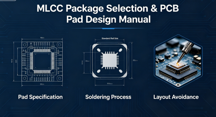
MLCC Package Selection & PCB Pad Design Manual: Pad Specification + Soldering Process + Layout Avoidance
mu sen Introduction
MLCC package selection and PCB pad design are critical to soldering reliability, electrical performance, and heat dissipation. Many failures such as solder detachment, ceramic cracking, poor contact, and high-frequency attenuation are caused by wrong packages, non-standard pads, or poor layout—not component quality.
MLCC packages (0402, 0603, 0805, 1206, 1210, etc.) differ greatly in current rating, heat dissipation, and parasitic parameters. Pad design directly affects solder strength, creepage distance, and ESL. The core logic: package matches application, pad matches package, layout balances performance and process.
This manual provides complete package characteristics, standard pad design, soldering rules, layout tips, real failure cases, and ready-to-use solutions to eliminate failures caused by improper package and pad design.
1. MLCC Package Characteristics & Selection Standards
Package naming: e.g., 0402 = length 0.04 inch, width 0.02 inch. Classified as miniature, standard, high-power/high-voltage.
1.1 Core Package Characteristics
| Package | Size (L×W mm) | Current | Heat Dissipation | ESL | Application | Cost |
|---|---|---|---|---|---|---|
| 0402 | 1.0×0.5 | ≤0.5A | Weak | ≤2nH | Wearable, Mobile | Medium |
| 0603 | 1.6×0.8 | ≤1A | Low | ≤3nH | Consumer, Charger | Low |
| 0805 | 2.0×1.25 | ≤2A | Medium | ≤5nH | Industrial, Automotive | Low |
| 1206 | 3.2×1.6 | ≤3A | Medium | ≤6nH | Industrial, HV | Low |
| 1210 | 3.2×2.5 | ≤5A | Strong | ≤8nH | HV, High Power | Medium |
| 1812 | 4.5×3.2 | ≤8A | Strong | ≤10nH | Industrial HV | Medium-High |
| 2220 | 5.6×5.0 | ≤10A | Very Strong | ≤12nH | Ultra-high Power | High |
1.2 Full‑Scenario Package Selection
- Consumer Miniature: 0402 / 0603
- General Consumer: 0603 / 0805
- General Industrial: 0805 / 1206
- Industrial HV / High Power: 1206 / 1210 / 1812
- Automotive: 0805 / 1206 / 1210 (avoid 0402)
- High Frequency: 0402 / 0603 / 0805 (avoid large packages)


2. MLCC Standard PCB Pad Design Specifications
2.1 Standard Pad Dimensions (mm)
| Package | Pad Length (L) | Pad Width (W) | Gap (S) | Solder Mask Opening |
|---|---|---|---|---|
| 0402 | 0.8~1.0 | 0.4~0.5 | 0.1~0.2 | 0.9×0.5 |
| 0603 | 1.2~1.4 | 0.6~0.8 | 0.2~0.3 | 1.3×0.7 |
| 0805 | 1.6~1.8 | 1.0~1.2 | 0.3~0.4 | 1.7×1.1 |
| 1206 | 2.8~3.0 | 1.4~1.6 | 0.4~0.5 | 2.9×1.5 |
| 1210 | 2.8~3.0 | 2.2~2.4 | 0.5~0.6 | 2.9×2.3 |
2.2 Critical Pad Design Taboos
- Pad too large / too small → bridging or weak soldering
- Insufficient gap → insufficient creepage, HV failure
- Wrong solder mask opening → poor soldering
- Sharp/irregular pads → electrical stress
- No isolation in HV → tracking risk
- Excessively long pads in HF → high ESL
2.3 Special Scenario Pad Optimization
- High Frequency: Short and wide pads, reduce ESL
- High Voltage: Increase gap + solder mask isolation
- Automotive Vibration: Wider pads + teardrop design
- High Temperature: Larger pads + thermal vias
3. MLCC Soldering Process Guidelines
3.1 Reflow Soldering
- Heating rate: ≤3℃/s
- Preheat: 150~180℃, 60~90s
- Peak: 240~260℃ (lead-free)
- Cooling rate: ≤2℃/s
3.2 Manual Soldering
- Iron temp: 320~350℃ (lead-free)
- Soldering time: ≤3s per side
- Do not press ceramic body
3.3 Soldering Quality Standard
- Smooth, full, no bridging, no cold solder
- No cracking, no electrode damage
- Stable mechanical strength
4. MLCC PCB Layout Rules & Avoidance Tips
- Spacing ≥0.5mm (general), ≥1mm (HV)
- Keep away from heat sources
- Place close to IC power pins
- Avoid PCB edges and corners
- HV section isolated from low voltage
4.1 Scenario Layout Optimization
- High Frequency: Short traces, minimize loop area
- High Voltage: Isolated layout, large clearance
- Automotive Vibration: Central PCB area, dual pads
- High Temperature: Good thermal relief, avoid dense placement
5. Real Failure Cases
Case 1: 0402 in automotive → vibration detachment
Fix: Replace with 0805 + teardrop pads
Case 2: Overly long pad in 6MHz GaN → high loss
Fix: Restore standard pad length, ESL <2nH
Case 3: Insufficient pad gap in 800V → tracking & flashover
Fix: Increase gap to 0.6mm + solder mask isolation
Case 4: Overheating soldering → ceramic cracking
Fix: 330℃, ≤3s per side
6. Common Misconceptions
Fact: Causes heat buildup, interference, and soldering issues
7. Package & Pad Design Checklist
- Package matches current, temperature, and space requirements
- Pad size, gap, solder mask follow standards
- HF: short pads; HV: increased gap; Automotive: teardrop
- Soldering temperature and time within limits
- Reasonable layout spacing, away from heat and noise
- Post-soldering inspection: appearance, electrical, mechanical
- No improper pad reduction or mismatched packages
- Automotive/HV: extra vibration and creepage checks
mu sen Conclusion
MLCC package and pad design directly determine product reliability. Core principles: package fits application, pad fits package, process ensures quality.
Most failures come from wrong selection, non-standard pads, or poor soldering—not component quality. Following this guide greatly improves reliability and reduces after-sales cost.
Dongguan Musen Leyton Electronic Technology Co., Ltd. provides full MLCC packages (0402~2220). We offer professional package selection, pad design templates, soldering suggestions, and free samples to optimize your design and enhance product reliability.
Contact Us
MLCC Failure Analysis Ultimate Troubleshooting Manual Complete Solutions for Cracking Breakdown Leakage Whistling Heating
MLCC Dielectric Selection Special Manual C0G / X5R / X7R / X8R Full Comparison Application Guide
Related Article