MLCC Parasitic Parameters Deep Analysis Optimization ESR/ESL/SRF Principle Measurement Circuit Impact Full-Link Resistance Reduction Solutions
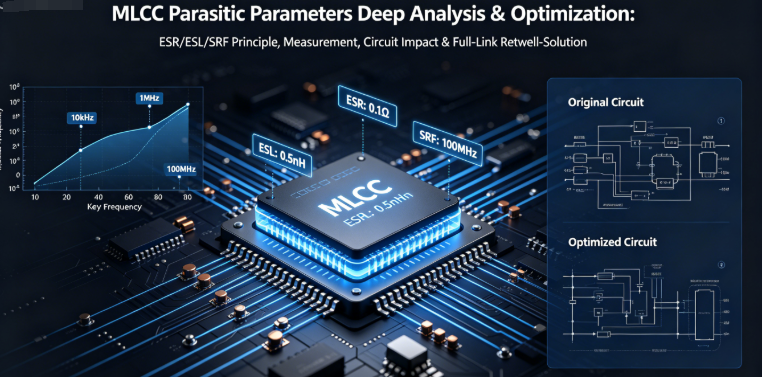
MLCC Parasitic Parameters Deep Analysis & Optimization: ESR/ESL/SRF Principle, Measurement, Circuit Impact & Full-Link Resistance Reduction Solutions
Company: Dongguan Musen Laidun Electronic Technology Co., Ltd.
Keywords: MLCC Parasitic Parameters, Equivalent Series Resistance ESR, Equivalent Series Inductance ESL, Self-Resonant Frequency SRF, Power Integrity PI, High-Frequency Filtering Optimization
Introduction
As electronic systems evolve toward higher frequencies, higher speeds, and lower-voltage high-current operation, MLCC parasitic parameters (ESR/ESL/SRF) have become the core factors determining circuit performance—often more important than nominal capacitance. Many engineers only focus on capacitance and voltage rating in design, ignoring parasitic effects, leading to intractable problems such as excessive power ripple, reduced switching efficiency, high-speed signal distortion, and EMI non-compliance.
MLCC is not an ideal pure capacitor. Its internal structure and external packaging inherently introduce Equivalent Series Resistance (ESR) and Equivalent Series Inductance (ESL). At low frequencies, capacitive reactance dominates impedance; when frequency rises above the Self-Resonant Frequency (SRF), inductive reactance exceeds capacitive reactance, and the capacitor behaves as an inductor, completely losing filtering function.
This article deeply analyzes the physical mechanism of MLCC's three major parasitic parameters and their comprehensive impact on circuit performance. It provides standardized measurement methods and full-link optimization solutions, combined with real cases from high-frequency power supplies, high-speed digital systems, and RF communications, helping engineers master parasitic parameter design and optimization skills to build high-performance, high-reliability electronic systems.
1. Physical Nature & Equivalent Model of MLCC Parasitic Parameters
1.1 Difference Between Ideal and Actual Capacitors
The impedance of an ideal capacitor decreases monotonically with frequency, following the formula: Z = 1/(2πfC). However, an actual MLCC is a complex network consisting of capacitance, resistance, and inductance, with the following equivalent circuit model:
- C: Nominal capacitance, determined by dielectric constant, electrode area, and dielectric thickness
- ESR (Equivalent Series Resistance): Includes dielectric loss resistance, internal electrode resistance, and terminal contact resistance
- ESL (Equivalent Series Inductance): Determined by internal electrode current paths, terminal structure, and external package lead inductance
- Rp (Equivalent Parallel Resistance): Represents dielectric leakage current, negligible at high frequencies
1.2 Impedance-Frequency Characteristic Curve
The total impedance of an actual MLCC is given by: Z = √[ESR² + (2πfESL - 1/(2πfC))²]
According to this formula, MLCC impedance changes with frequency in three stages:
- Capacitive Region (f < SRF): Capacitive reactance dominates, impedance decreases with frequency, capacitor acts as a capacitor with filtering function
- Resonant Point (f = SRF): Capacitive and inductive reactance cancel each other, total impedance equals ESR, reaching minimum value
- Inductive Region (f > SRF): Inductive reactance dominates, impedance increases with frequency, capacitor acts as an inductor, losing filtering function
1.3 Generation Mechanism of Three Major Parasitic Parameters
1.3.1 ESR (Equivalent Series Resistance)
- Dielectric Loss: Polarization loss of ceramic dielectric under alternating electric field, related to dielectric type and frequency. X5R/X7R have higher dielectric loss than C0G
- Electrode Loss: Metal resistance of internal and terminal electrodes, related to material, thickness, and area
- Contact Loss: Contact resistance between terminal and pad, related to soldering quality
1.3.2 ESL (Equivalent Series Inductance)
- Internal Inductance: Inductance generated by current flowing through multi-layer internal electrodes, related to number of layers and current path length
- External Inductance: Inductance from terminals and package leads, related to package size and shape
- Mounting Inductance: Inductance from PCB pads and traces, typically accounting for over 50% of total ESL
1.3.3 SRF (Self-Resonant Frequency)
SRF is the critical point where a capacitor transitions from capacitive to inductive behavior, calculated as: SRF = 1/(2π√(C×ESL))
SRF is inversely proportional to capacitance and ESL: larger capacitance and higher ESL result in lower SRF; smaller capacitance and lower ESL result in higher SRF.
2. Comprehensive Impact of Parasitic Parameters on Circuit Performance
2.1 Impact on Power Filtering Performance
- High-Frequency Ripple Suppression Failure: When power noise frequency exceeds SRF, the capacitor becomes inductive and cannot effectively filter high-frequency ripple
- Increased Power Impedance: ESR and ESL increase power output impedance, leading to poor load transient response and larger voltage droop
- Increased Heating Loss: ESR converts electrical energy into heat, raising capacitor temperature, accelerating aging, and potentially causing thermal breakdown
2.2 Impact on High-Speed Digital Circuits
- Signal Integrity Issues: Excessive ESL in power decoupling capacitors increases power noise, causing signal jitter and bit errors
- Ground Bounce Noise: High-speed switching current flowing through ESL generates voltage spikes (ground bounce), interfering with adjacent circuits
- Timing Deviation: Power supply voltage fluctuations change gate circuit propagation delay, causing timing errors
2.3 Impact on Switching Power Supply Performance
- Reduced Conversion Efficiency: ESR and ESL increase switching and conduction losses, lowering power supply efficiency
- Poor Loop Stability: Parasitic parameters change power supply loop gain and phase margin, leading to loop oscillation
- Increased Output Ripple: ESR causes larger output voltage ripple, affecting normal load operation
2.4 Impact on EMI Electromagnetic Compatibility
- Radiated Emission Non-Compliance: High-frequency current flowing through ESL generates electromagnetic radiation, causing radiated emission超标
- Conducted Emission Non-Compliance: High-frequency noise on power lines cannot be effectively filtered, leading to conducted emission超标
- Reduced Anti-Interference Ability: Parasitic parameters reduce the circuit's ability to suppress external electromagnetic interference
3. Standardized Measurement Methods for MLCC Parasitic Parameters
3.1 Measurement Equipment Selection
| Measurement Equipment | Frequency Range | Measurable Parameters | Application Scenario |
|---|---|---|---|
| LCR Meter | 20Hz~1MHz | C, ESR | Low-frequency parameter measurement |
| Impedance Analyzer | 100Hz~40GHz | C, ESR, ESL, SRF, Impedance-Frequency Curve | Full-band parasitic parameter measurement |
| Network Analyzer | 9kHz~110GHz | S-Parameters, Impedance-Frequency Curve | High-frequency and RF parameter measurement |
3.2 Measurement Precautions
- Fixture Calibration: Perform open, short, and load calibration before measurement to eliminate fixture parasitic effects
- Frequency Matching: Measurement frequency should match the actual operating frequency of the capacitor; otherwise, results are meaningless
- Temperature Control: Parasitic parameters vary significantly with temperature; maintain ambient temperature at 25℃±5℃ during measurement
- Sample Preparation: Samples should be free of oxidation and damage, with good soldering quality to avoid contact resistance interference
3.3 Typical Parasitic Parameter Reference Values
| Package Size | Typical ESL Value | Typical ESR Value (1MHz) | Typical SRF Value (1μF) |
|---|---|---|---|
| 0402 | 0.5~1nH | 5~10mΩ | 10~15MHz |
| 0603 | 1~2nH | 3~8mΩ | 5~10MHz |
| 0805 | 2~3nH | 2~5mΩ | 3~5MHz |
| 1206 | 3~5nH | 1~3mΩ | 1~3MHz |
4. Full-Link Optimization Solutions for MLCC Parasitic Parameters
4.1 Selection Optimization: Reduce Parasitics at the Source
- Prefer Smaller Packages: Smaller package size means lower ESL; 0402 package has approximately 1/3 the ESL of 1206 package
- Use Low ESR/ESL Special Dielectrics: C0G dielectric has much lower ESR than X7R/X8R; high-frequency optimized X8R dielectrics offer lower ESR and ESL
- Select Special Structure MLCCs:
- Reverse Termination MLCC: Shortens current path, reduces ESL by 30%~50%
- Array MLCC: Multiple capacitors integrated in one package, lower total ESL
- Embedded MLCC: Directly embedded in PCB, eliminates mounting inductance
4.2 Layout Optimization: Minimize Mounting Inductance
- Place Close to Power Pins: Decoupling capacitors should be as close as possible to the chip's power and ground pins to minimize current loop length
- Short Trace Length: Trace length from capacitor to power and ground should be less than 1mm to avoid additional inductance from long traces
- Increase Via Count: Use 2~4 vias per capacitor for power and ground connections to reduce via inductance
- Use Short, Wide Traces: Traces should be short and wide (≥0.2mm width) to reduce trace resistance and inductance
4.3 Routing Optimization: Reduce Loop Inductance
- Adjacent Power and Ground Planes: Tightly coupled power and ground planes form a low-impedance plane, reducing power distribution inductance
- Minimize Loop Area: Power current outflow and return paths should be as close as possible to reduce loop area
- Avoid Split Power Planes: Split power planes increase current path length and introduce additional inductance
- Use Ground Plane as Return Path: All signal and power return currents should flow through the ground plane to avoid long return paths
4.4 Combined Filtering Optimization: Cover Full-Band Noise
A single capacitor can only effectively filter noise in a specific frequency band. Using a combination of capacitors with different capacitances and packages can cover full-band noise from low to high frequencies:
- Large capacitance (10μF~100μF): Filters low-frequency ripple (10kHz~1MHz)
- Medium capacitance (0.1μF~1μF): Filters mid-frequency noise (1MHz~10MHz)
- Small capacitance (1nF~100nF): Filters high-frequency noise (10MHz~100MHz)
- Ultra-small capacitance (100pF~1nF): Filters ultra-high-frequency noise (above 100MHz)
Note: Capacitors should be placed from farthest to closest to the chip in order of decreasing capacitance to prevent high-frequency noise from being blocked by the ESL of large capacitors.
4.5 Process Optimization: Reduce Contact Resistance
- Optimize Soldering Process: Use reflow soldering, control temperature and time to ensure good soldering quality
- Use Lead-Free Solder: Lead-free solder has better conductivity and lower contact resistance
- Avoid Cold Solder and Dewetting: Cold solder and dewetting cause sharp increases in contact resistance and ESR
5. Typical Scenario Parasitic Parameter Cases & Rectification
Case 1: Excessive High-Frequency Ripple in GaN Fast Charger
Problem: 65W GaN fast charger output ripple exceeded 50mV specification, reaching 120mV
Root Cause: Output filter capacitor used 1206 package 10μF X7R with SRF only 2MHz, unable to filter 10MHz high-frequency ripple generated by GaN switching
Solution: Replace 1×1206 10μF with 2×0603 4.7μF + 1×0402 100nF combined filtering, reducing total ESL by 60% and increasing SRF to 15MHz
Result: Output ripple reduced to 35mV, meeting specifications; power efficiency improved by 0.5%


Case 2: Bit Errors Caused by High-Speed FPGA Power Noise
Problem: High-speed FPGA (1GHz operating frequency) experienced random bit errors during data transmission, with bit error rate ~10^-9
Root Cause: FPGA power pin decoupling capacitors were placed too far away, with 5mm trace length introducing ~5nH additional inductance, resulting in 150mV power noise
Solution: Place decoupling capacitors directly adjacent to FPGA pins, reduce trace length to 0.5mm, add 2 vias per capacitor, lowering total mounting inductance to below 1nH
Result: Power noise reduced to 30mV, bit error rate dropped to 0, system stability significantly improved
Case 3: Switching Power Supply EMI Radiated Emission Non-Compliance
Problem: 100W switching power supply exceeded GB 9254 standard by 6dB in the 30MHz~100MHz frequency band
Root Cause: Excessive ESL in input filter capacitors prevented effective filtering of high-frequency switching noise, which radiated through power lines
Solution: Add 1×0402 10nF C0G capacitor in parallel with the existing 10μF electrolytic capacitor to form a low-pass filter network
Result: Radiated emission in 30MHz~100MHz band reduced by 8dB, meeting standard requirements
6. Common Misconceptions & Pitfalls
- Misconception 1: Larger capacitance = better filtering → Truth: Large capacitors have low SRF and poor high-frequency filtering; must be used with small capacitors
- Misconception 2: Lower ESR is always better → Truth: Excessively low ESR may cause power supply loop instability; select appropriate ESR based on loop design
- Misconception 3: SRF above operating frequency is sufficient → Truth: Impedance already rises near SRF, reducing filtering effect; select capacitors with SRF 2~3 times higher than operating frequency
- Misconception 4: Parallel identical capacitors reduce ESL → Truth: Parallel identical capacitors only reduce ESR, with limited effect on ESL; use combinations of different capacitances and packages
- Misconception 5: Parasitic parameters only affect high-frequency circuits → Truth: Even in low-frequency circuits, ESR causes heating and efficiency reduction, affecting system reliability
7. Parasitic Parameter Optimization Design Checklist
- Selection: Prefer small packages, low ESR/ESL special dielectrics, and special structure MLCCs
- Layout: Decoupling capacitors directly adjacent to chip power pins, trace length ≤1mm
- Routing: Adjacent power and ground planes, minimize current loop area, avoid split power planes
- Filtering: Use multi-capacitance, multi-package combinations to cover full-band noise
- Vias: Use 2~4 vias per capacitor to reduce via inductance
- Measurement: Use impedance analyzer to measure parasitic parameters at actual operating frequency
- Verification: Validate optimization effects through power integrity simulation and actual testing
- Process: Optimize soldering process to ensure good quality and reduce contact resistance
mu sen Conclusion
In high-frequency high-speed electronic systems, MLCC parasitic parameters have become the key factor determining system performance. Engineers must fundamentally understand the generation mechanisms of ESR, ESL, and SRF and their impact on circuits, mastering full-link optimization methods from selection, layout, routing to process.
The core of parasitic parameter optimization is "minimizing impedance": by selecting low-parasitic capacitors, optimizing layout and routing, and adopting combined filtering architectures, maintain low power supply impedance across the entire operating frequency band. Only in this way can we effectively filter noise, improve power efficiency, ensure signal integrity, and meet EMC requirements.
Dongguan Musen Leyton Electronic Technology Co., Ltd. provides a full range of low ESR/ESL MLCC products, including high-frequency special types, reverse termination types, and array types, meeting parasitic parameter optimization needs in different scenarios. We also provide professional power integrity simulation and parasitic parameter testing services to help customers solve challenges in high-frequency high-speed design.
MLCC Power Integrity PI Special Design White Paper PDN Impedance Target Decoupling Capacitance Calculation Full-Band Filtering High-Speed System Power Design
MLCC 9 Failure Modes Troubleshooting Manual Full Symptoms Root Cause Analysis Permanent Solutions Quick Reference
Related Article