MLCC Special Application in SiC GaN Third-Generation Semiconductors High-Frequency High-dv dt Challenges Dielectric Loss Optimization Low-ESL Design High-Reliability Selection Solutions
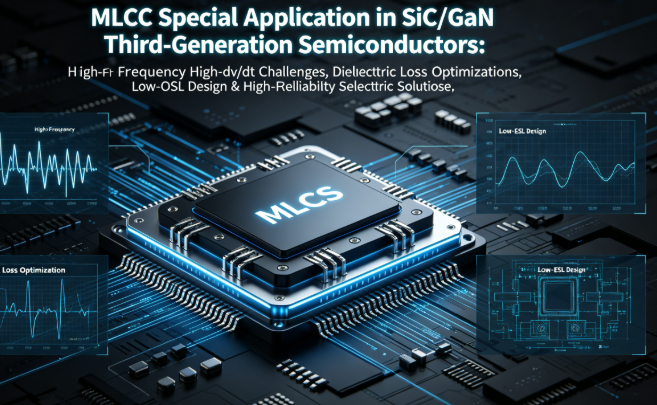
MLCC Special Application in SiC/GaN Third-Generation Semiconductors: High-Frequency High-dv/dt Challenges, Dielectric Loss Optimization, Low-ESL Design & High-Reliability Selection Solutions
Company: Dongguan Musen Laidun Electronic Technology Co., Ltd.
Keywords: SiC MLCC, GaN Capacitor, Third-Generation Semiconductors, High dv/dt Tolerance, High-Frequency Low-Loss, Low-ESL Capacitor, Silicon Carbide Inverter, Gallium Nitride Fast Charger
mu sen introduction
Third-generation semiconductors represented by Silicon Carbide (SiC) and Gallium Nitride (GaN) are completely disrupting the traditional silicon-based power device market with their excellent characteristics: wide bandgap, high breakdown field strength, high electron mobility, and high temperature resistance. SiC has become standard for new energy vehicles, PV energy storage, and industrial inverters, while GaN is rapidly gaining popularity in fast chargers, consumer electronics power supplies, and data center power supplies. The switching frequency of third-generation semiconductors has increased from 20~100kHz (traditional silicon) to 100kHz~1MHz, switching speed has increased by more than 10 times, and dv/dt can reach 100V/ns or even higher, posing unprecedented stringent requirements for supporting MLCCs.
Traditional silicon-era MLCC selection logic is completely unsuitable for third-generation semiconductor scenarios. Extensive engineering practice shows that SiC/GaN power supplies using ordinary MLCCs generally suffer from capacitor overheating burnout, excessive high-frequency ripple, excessive switching spikes, severe EMI, and drastically reduced lifespan, even leading to mass explosion accidents. The core reason is that engineers ignore the special failure mechanisms of MLCC under high-frequency high-dv/dt conditions, as well as new requirements for parasitic parameters, dielectric loss, and voltage tolerance.
This whitepaper is the industry's first special MLCC application guide for third-generation semiconductors. It deeply analyzes five core challenges of SiC/GaN systems for MLCC, reveals special failure mechanisms under high-frequency high-dv/dt, provides standardized dielectric selection, package selection, derating specifications, and PCB layout routing solutions. Combined with typical scenarios such as SiC automotive inverters, GaN fast chargers, and PV energy storage converters, it provides actionable high-reliability design solutions to help engineers build efficient, stable, and long-life third-generation semiconductor power systems.
1. Five Core Challenges of Third-Generation Semiconductors for MLCC
1.1 Extremely High dv/dt Impact Challenge
SiC/GaN devices have extremely fast switching speeds, with voltage rise edge dv/dt reaching 50~200V/ns, 5~20 times that of traditional IGBTs. Such a high voltage change rate generates extremely strong displacement current inside MLCC, causing three major problems:
- Electric field concentration at electrode edges, leading to local breakdown and accelerated dielectric aging
- Excessive displacement current, causing capacitor heating and increased loss
- Generating strong electromagnetic radiation, leading to EMI non-compliance
1.2 High-Frequency Dielectric Loss Challenge
When switching frequency increases above 100kHz, MLCC dielectric loss becomes an important part of total system loss. Traditional X7R dielectric loss increases sharply at high frequencies, causing severe self-heating of capacitors, which not only reduces power supply efficiency but also accelerates dielectric aging and shortens service life. At 1MHz frequency, the loss of ordinary X7R is 3~5 times that of high-frequency special dielectric.
1.3 Parasitic Parameter Sensitivity Challenge
At high frequencies, the impact of MLCC's Equivalent Series Inductance (ESL) and Equivalent Series Resistance (ESR) on circuit performance is dramatically amplified. Even a few nH of ESL will generate significant voltage spikes under high dv/dt, leading to overvoltage breakdown of switching tubes; excessive ESR increases heating and loss, reducing system efficiency.
1.4 High-Temperature Operating Environment Challenge
The maximum operating temperature of SiC devices can reach 175℃~200℃, much higher than 125℃ of traditional silicon devices. This requires supporting MLCCs to operate stably for a long time above 150℃ while maintaining good electrical performance and reliability. Ordinary X7R dielectric will experience severe capacitance decay and accelerated aging above 125℃.
1.5 High Reliability & Long Life Challenge
SiC/GaN are mainly used in fields with extremely high reliability requirements such as new energy vehicles, PV energy storage, and industrial control, requiring product life of more than 15 years. Under the superposition of multiple stresses of high frequency, high temperature, and high dv/dt, MLCC life will be significantly shortened, requiring higher reliability design and materials.
2. Special MLCC Failure Mechanisms Under High-Frequency High-dv/dt
2.1 Edge Electric Field Breakdown Failure
Under high dv/dt impact, extremely strong electric field concentration occurs at the edges of MLCC internal electrodes, with electric field strength reaching 5~10 times the average electric field. When the local electric field exceeds the dielectric breakdown field strength, edge breakdown occurs, forming a conductive channel and eventually leading to capacitor short circuit failure. This failure mode is particularly common in ordinary high-voltage MLCCs, and is sudden and batch-wise.
2.2 High-Frequency Dielectric Thermal Runaway Failure
The loss of Class II dielectrics increases with frequency, and the heat generated by loss increases capacitor temperature, which in turn further increases dielectric loss, forming a positive feedback loop. When heat dissipation is poor, dielectric thermal runaway occurs, eventually leading to capacitor burnout. This failure mode is particularly prominent in high-density power supplies such as GaN fast chargers.
2.3 Voltage Transient Fatigue Failure
Periodic voltage transients generated by high-frequency switching cause repeated electrical stress impacts on MLCC dielectric, leading to micro-cracks and defects inside the dielectric. Over time, these defects gradually expand, eventually leading to dielectric breakdown. This failure mode has a cumulative effect and usually breaks out intensively months to years after product use.
2.4 Secondary Failures Caused by Parasitic Parameters
MLCC's ESL resonates with parasitic inductance in the circuit, amplifying voltage spikes and causing overvoltage breakdown of switching tubes; at the same time, displacement current under high dv/dt couples to the control circuit through parasitic capacitance, causing false triggering and system crashes. These secondary failures caused by MLCC parasitic parameters are often more destructive than capacitor self-failure.
3. Special MLCC Selection Standards for SiC/GaN
3.1 Dielectric Selection: High-Frequency Low-Loss is Core
| Dielectric Type | tanδ at 1MHz | Max Operating Temp | dv/dt Tolerance | Application Scenarios |
|---|---|---|---|---|
| C0G/NPO | ≤0.001 | 150℃ | Extremely High (≥200V/ns) | High-frequency snubber, resonant circuits, precision sampling |
| High-Frequency Special X8R | ≤0.01 | 150℃ | High (≥100V/ns) | DC-Link filtering, output filtering, snubber circuits |
| Ordinary X7R | ≤0.03 | 125℃ | Medium (≤50V/ns) | Only for low-frequency scenarios below 100kHz |
| X5R | ≤0.05 | 85℃ | Low (≤30V/ns) | Prohibited in SiC/GaN systems |
Selection Iron Rule: In SiC/GaN systems, X5R dielectric is prohibited; C0G and high-frequency special X8R dielectrics are preferred; high-frequency low-loss dielectrics must be used for frequencies above 100kHz.
3.2 Package Selection: Small Package + Special Structure First
- Prefer small packages: Smaller package = lower ESL = better high-frequency performance. 0402/0603 packages are preferred, maximum not exceeding 0805
- Reverse termination MLCC: Optimizes electrode structure to reduce ESL by 30%~50%, especially suitable for high-frequency snubber circuits
- Array MLCC: Multiple capacitors integrated in one package, lower total ESL, saves PCB space
- Thick dielectric high-voltage MLCC: Adopts thickened dielectric layer and edge electric field optimization design, significantly improves dv/dt tolerance
3.3 Voltage Derating Standards: Stricter Than Traditional Systems
Due to high dv/dt and high-frequency transient voltage, MLCC voltage derating in SiC/GaN systems must be stricter than traditional silicon-based systems:
| Application Scenario | DC Steady-State Voltage Derating | Peak Voltage Derating | Remarks |
|---|---|---|---|
| GaN Consumer Fast Charger | ≥2.0x | ≥2.5x | High density, high heating scenario |
| SiC Automotive Inverter | ≥2.5x | ≥3.0x | High reliability, 15-year life requirement |
| PV Energy Storage Converter | ≥2.5x | ≥3.0x | Outdoor harsh environment, 25-year life |
| Snubber Absorption Circuit | ≥3.0x | ≥4.0x | Withstands extremely high dv/dt impact |
3.4 Temperature Derating Standards: Sufficient Temperature Margin
- C0G dielectric: Max operating temp 150℃, recommended operating temp ≤125℃
- High-frequency X8R dielectric: Max operating temp 150℃, recommended operating temp ≤125℃
- Ordinary X7R dielectric: Max operating temp 125℃, recommended operating temp ≤100℃
- In any case, MLCC operating temperature should not exceed 80% of its maximum rated temperature
4. Key PCB Design Specifications for SiC/GaN Systems
4.1 Layout Principles: Minimize Current Loop
- MLCC must be as close as possible to the drain and source of switching tubes to shorten current loop length
- Snubber capacitors should be directly connected across the drain-source of switching tubes, trace length ≤0.5mm
- DC-Link capacitors should be evenly distributed around the power loop, avoid concentrated layout
- Strictly isolate high-voltage loops from low-voltage control loops to avoid electromagnetic interference
4.2 Routing Principles: Minimize Parasitic Parameters
- Power loop traces should be short and wide, width ≥2mm, thickness ≥2oz, to reduce trace resistance and inductance
- Use 2~4 vias per MLCC for power and ground connections, via diameter ≥0.3mm, to reduce via inductance
- Avoid right-angle and acute-angle traces, use 45-degree or arc transitions
- Power and ground planes should be closely adjacent, dielectric thickness ≤0.2mm, to increase planar capacitance and reduce plane impedance
4.3 Thermal Design: Avoid Capacitor Overheating
- MLCC should be kept away from heat sources such as switching tubes, inductors, and transformers
- Add thermal via arrays under MLCC to conduct heat to the ground plane
- Use multiple small-capacity capacitors in parallel instead of single large-capacity capacitors to disperse heat
- For high-density power supplies, consider heat sinks or forced air cooling
5. Typical Scenario Application Solutions
5.1 65W GaN Fast Charger Adapter
Core Challenges: High power density, high switching frequency (100~300kHz), poor heat dissipation, cost sensitivity
Selection Solution:
- Primary high-voltage filtering: 0805 10μF 400V High-Frequency X8R
- Switch tube snubber: 0603 1nF 630V C0G
- Secondary output filtering: 0603 22μF 25V High-Frequency X8R + 0402 100nF C0G
Design Points: Use multiple small-capacity capacitors in parallel, optimize layout and routing to minimize parasitic parameters; strengthen thermal design to avoid capacitor overheating.
Result: Power efficiency increased by 1%, temperature reduced by 5℃, EMI meets Class B standard.
5.2 800V SiC Automotive Inverter
Core Challenges: High voltage (800V), high dv/dt (100V/ns), high temperature (125℃), high reliability requirement (15 years/200,000 km)
Selection Solution:
- DC-Link filtering: 1206 1μF 2000V Thick Dielectric High-Frequency X8R × 24 parallel
- IGBT snubber: 0805 10nF 1500V C0G
- Drive power filtering: 0603 1μF 100V High-Frequency X8R + 0402 10nF C0G
Design Points: Adopt voltage derating above 2.5x; use thick dielectric high-dv/dt tolerant capacitors; optimize thermal design to control capacitor operating temperature below 105℃.
Result: Passed 1000-hour high-temperature high-voltage aging test with no failures; system efficiency increased by 2%, temperature rise reduced by 10℃.
5.3 1500V PV Energy Storage Converter
Core Challenges: Ultra-high voltage (1500V), outdoor harsh environment, 25-year life requirement, frequent grid fluctuations
Selection Solution:
- DC bus filtering: 1210 0.47μF 3000V High-Frequency X8R × 36 parallel
- AC output filtering: 0805 0.1μF 1000V C0G
- Auxiliary power filtering: 0603 10μF 100V High-Frequency X8R
Design Points: Adopt voltage derating above 3x; use anti-sulfur and moisture-proof MLCC; PCB strictly implements high-voltage creepage distance standards; full-board conformal coating.
Result: Passed 2000-hour high-temperature high-humidity aging test, capacitance decay ≤5%; meets 25-year service life requirement.
6. Common Misconceptions & Pitfalls
- Misconception 1: Ordinary MLCC can be used in SiC/GaN systems as long as voltage rating is sufficient → Truth: Ordinary MLCC's dv/dt tolerance and high-frequency loss cannot meet requirements, leading to overheating burnout and early failure
- Misconception 2: Larger capacitance = better filtering → Truth: Large capacitors have higher ESL and ESR, poor high-frequency filtering, and more severe heating; use multiple small capacitors in parallel
- Misconception 3: X7R and X8R have similar performance and can be interchanged → Truth: Ordinary X7R has much higher loss than high-frequency special X8R at high frequency and high temperature, leading to thermal runaway in long-term use
- Misconception 4: Parasitic parameters only affect EMI, not reliability → Truth: Excessive ESL generates fatal voltage spikes, causing breakdown of switching tubes and capacitors
- Misconception 5: Derating standards are the same as traditional silicon systems → Truth: Transient voltage and dv/dt in SiC/GaN systems are much higher than traditional systems, requiring stricter derating standards
7. SiC/GaN MLCC Design Checklist
- All MLCCs use C0G or high-frequency special X8R dielectric, X5R prohibited
- Prefer 0402/0603 small packages, maximum not exceeding 0805
- DC steady-state voltage derating ≥2.0x, peak voltage derating ≥2.5x
- Snubber absorption circuit voltage derating ≥3.0x
- MLCC operating temperature ≤80% of maximum rated temperature
- Capacitors as close as possible to switching tubes, trace length ≤0.5mm
- Use 2~4 vias per capacitor to reduce via inductance
- Power loop traces short and wide, width ≥2mm
- Power and ground planes closely adjacent, dielectric thickness ≤0.2mm
- Optimize thermal design to avoid capacitor overheating
- Perform high-frequency impedance simulation to ensure full-band impedance meets requirements
- Perform high-temperature high-voltage aging test to verify long-term reliability
mu sen Conclusion
The rapid development of third-generation semiconductors is driving revolutionary changes in power technology, while also putting forward new requirements for supporting passive components. As the core passive component in power systems, MLCC performance directly determines the efficiency, reliability, and service life of SiC/GaN systems. Traditional MLCC selection and design methods can no longer adapt to the new working conditions of high-frequency high-dv/dt, and MLCC products and design solutions specially optimized for third-generation semiconductors must be adopted.
When designing SiC/GaN systems, engineers should focus on MLCC's high-frequency loss, dv/dt tolerance, parasitic parameters, and high-temperature reliability, following the design principles of "high-frequency low-loss dielectric, small package, high derating, short traces". Only by comprehensive optimization from selection, layout, routing to heat dissipation can we fully leverage the performance advantages of third-generation semiconductors and create efficient, stable, and long-life power products.
Dongguan Musen Leyton Electronic Technology Co., Ltd. provides a full range of SiC/GaN special MLCC products, including high-frequency low-loss C0G/X8R series, thick dielectric high-dv/dt series, reverse termination low-ESL series, and array MLCC, covering 63V~3000V full voltage range, meeting the needs of different scenarios such as GaN fast chargers, SiC inverters, and PV energy storage. We also provide professional power integrity simulation and design services to help customers solve challenges in third-generation semiconductor power design.
High-Reliability MLCC Application in Medical Electronics Medical Grade Certification System Biocompatibility Sterilization Resistance Ultra-Low Leakage Full-Scenario Selection Solutions
We also have a large stock of popular Yageo Huake Sanhuan Samsung and Lexy capacitors all at competitive prices Genuine original products
Related Article