MLCC Power Integrity PI Special Design White Paper PDN Impedance Target Decoupling Capacitance Calculation Full-Band Filtering High-Speed System Power Design
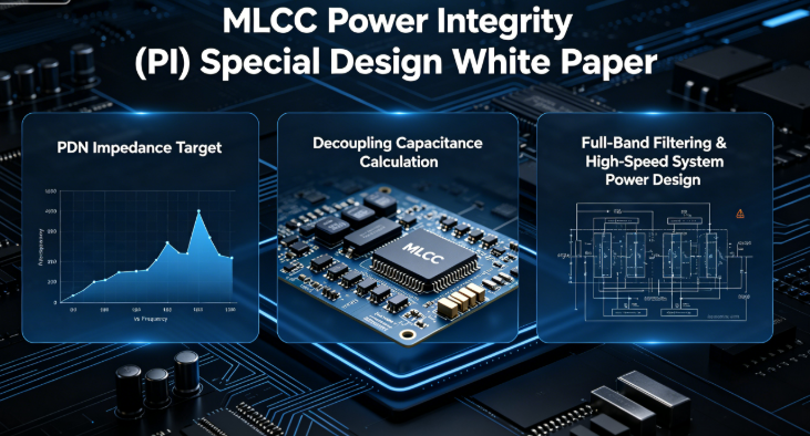
MLCC Power Integrity (PI) Special Design White Paper: PDN Impedance Target, Decoupling Capacitance Calculation, Full-Band Filtering & High-Speed System Power Design
Company: Dongguan Musen Laidun Electronic Technology Co., Ltd.
Power Integrity PI, PDN Power Distribution Network, Target Impedance Method, Decoupling Capacitor Calculation, MLCC Decoupling Design, High-Speed Power Design
mu sen Introduction
As semiconductor process advances to 7nm and 5nm, chip operating voltage continues to drop (below 0.8V), while operating current surges (hundreds of amps per chip), and switching frequency exceeds GHz level. This makes Power Integrity (PI) one of the most challenging issues in high-speed electronic system design, directly determining system stability, reliability, and performance limits.
As the core decoupling component in the Power Distribution Network (PDN), MLCC plays a critical role in providing instantaneous current to chips, suppressing power noise, and maintaining stable voltage. Over 90% of the performance of a well-designed PDN system depends on MLCC selection, quantity, layout, and routing. Many issues in high-speed systems such as signal jitter, bit errors, crashes, and EMI non-compliance root in improper MLCC decoupling design.
This article systematically explains core PI theories, PDN impedance target setting methods, accurate decoupling capacitor calculation models, MLCC decoupling design principles, layout and routing optimization techniques. Combined with practical cases of high-speed processors, FPGAs, DDR memory, it provides actionable PI design flows and specifications to help engineers build low-impedance, high-stability PDN.
1. Basic PI Theory & PDN Architecture
1.1 Definition & Importance of Power Integrity
Power Integrity refers to the ability of the power system to maintain chip power pin voltage within specified limits under dynamic load changes. Ideally, chip power pin voltage is constant DC voltage. In practice, due to PDN impedance, rapid current changes from chips cause voltage drops and fluctuations (power noise).
Hazards of Power Noise:
- Cause chip timing errors, bit errors, crashes, and restarts
- Reduce chip operating frequency and limit system performance
- Increase chip power consumption and heating
- Generate electromagnetic radiation leading to EMI non-compliance
- Accelerate chip aging and reduce system lifespan
1.2 PDN Composition
A complete PDN system from power module to chip power pins includes:
- Voltage Regulator Module (VRM): Converts input voltage to chip operating voltage, provides steady DC current
- High-capacity energy storage capacitors: Electrolytic/tantalum capacitors, filter low-frequency ripple, provide millisecond-level instantaneous current
- Medium-capacity decoupling capacitors: MLCC, filter mid-frequency noise, provide microsecond-level instantaneous current
- Small-capacity high-frequency decoupling capacitors: Small-package MLCC, filter high-frequency noise, provide nanosecond-level instantaneous current
- PCB power & ground planes: Form low-impedance paths for current transmission
- Chip package & pads: Connect PCB and internal chip power network
1.3 PDN Impedance & Frequency Response
PDN impedance is a function of frequency, dominated by different components in each band:
- Low-frequency (DC~10kHz): VRM output impedance
- Mid-frequency (10kHz~1MHz): High-capacity energy storage capacitors
- High-frequency (1MHz~100MHz): MLCC decoupling capacitors
- Ultra-high-frequency (>100MHz): PCB power/ground plane impedance + chip package impedance
Core PI Goal: Control PDN impedance below target impedance across the full chip operating frequency range.
2. Target Impedance Method: Golden Rule of PDN Design
2.1 Definition & Calculation of Target Impedance
Target Impedance (Ztarget) is the maximum allowable PDN impedance, determined by chip voltage, voltage tolerance, and maximum dynamic current:
Ztarget = (Vcore × Vtolerance) / Imax
- Vcore: Chip core operating voltage
- Vtolerance: Maximum allowable voltage fluctuation (typically ±5% or ±3%)
- Imax: Maximum dynamic current change of the chip
2.2 Typical Chip Target Impedance Reference
| Chip Type | Operating Voltage (V) | Voltage Tolerance | Max Dynamic Current (A) | Target Impedance (mΩ) |
|---|---|---|---|---|
| Standard MCU | 3.3 | ±5% | 0.5 | 330 |
| ARM Processor | 1.8 | ±5% | 2 | 45 |
| Mid/High-End FPGA | 1.0 | ±3% | 10 | 3 |
| High-Performance CPU | 0.8 | ±2.5% | 50 | 0.4 |
| DDR5 Memory | 1.1 | ±3% | 20 | 1.65 |
2.3 Target Impedance Design Flow
- Determine operating voltage, tolerance, and max dynamic current per chip datasheet
- Calculate target impedance Ztarget
- Design PDN system and select capacitor combination + layout
- Simulate PDN impedance-frequency curve
- Optimize design to ensure impedance < Ztarget across full frequency range
- Build prototype and test power noise & impedance
3. Accurate MLCC Decoupling Calculation
3.1 Single MLCC Impedance Model
Impedance of a single MLCC is determined by C, ESR, ESL:
Z = √[ESR² + (2πfESL - 1/(2πfC))²]
At SRF, capacitive and inductive reactance cancel; minimum impedance Zmin = ESR.
3.2 Parallel MLCC Impedance Characteristics
- Total Capacitance: Ctotal = N × C
- Total ESR: ESRtotal = ESR / N
- Total ESL: ESLtotal ≈ ESL / √N (layout-dependent)
- SRF: Remains unchanged
3.3 Frequency Coverage of MLCC Capacitance
| Capacitance | Typical Package | Typical SRF | Effective Filter Band |
|---|---|---|---|
| 10μF | 0805 | 2~3MHz | 100kHz~5MHz |
| 1μF | 0603 | 5~10MHz | 1MHz~20MHz |
| 0.1μF | 0402 | 15~20MHz | 5MHz~50MHz |
| 10nF | 0402 | 50~80MHz | 20MHz~100MHz |
| 1nF | 0402 | 150~200MHz | 100MHz~300MHz |
| 100pF | 0402 | 500~800MHz | 300MHz~1GHz |
3.4 Decoupling Capacitor Quantity Calculation
Minimum quantity based on target impedance:
N ≥ ESR / Ztarget
Note: This is theoretical minimum. Add 20%~30% margin in practice and account for layout/routing extra impedance.
4. MLCC Selection & Layout Principles
4.1 MLCC Selection Rules
- Prefer small packages: Smaller package = lower ESL = better high-frequency decoupling (0402 is preferred for high-speed design)
- Use low-ESR dielectrics: C0G (lowest) > X8R > X7R > X5R; prioritize C0G/high-frequency X8R
- Reasonable capacitance combination: "Large + Medium + Small" for full-band coverage
- Avoid over-sized capacitors: Low SRF, poor high-frequency performance, higher cost/space
- Unified package: Same package for one power domain for easier layout & production
4.2 MLCC Layout Rules
- Place close to power pins: Ideal distance < 0.5mm
- Small first, large later: Small high-frequency caps closest to pins
- Symmetric layout: Evenly distribute around chips, avoid one-side concentration
- At least one cap per power pin: 0.1μF for high-speed chips
- No shared vias: Independent vias for power/ground of each capacitor
4.3 MLCC Routing Rules
- Shortest path: Trace length < 1mm
- Widest traces: Width > 0.2mm to reduce resistance/inductance
- Direct connection: Cap to power/ground pins directly
- Via optimization: Multiple parallel vias, large diameter, smooth walls
- Avoid right angles: Use 45° or arc traces to reduce EMI
5. Multi-Layer PCB Power & Ground Plane Design
5.1 Functions of Power & Ground Planes
- Provide low-impedance current paths
- Form planar capacitance for ultra-high-frequency decoupling
- Shield EMI and reduce radiation
- Provide reference planes for signal integrity
5.2 Stack-Up Design Rules
- Adjacent power & ground planes: Thin dielectric for maximum planar capacitance & lowest impedance
- Multiple power domain分割: Split gap > 0.5mm
- Continuous ground plane: No分割 or slots to avoid increased impedance
- Symmetric stack-up: Reduce PCB warpage
5.3 Planar Capacitance Calculation
Cplane = (εr × ε0 × A) / d
- εr: Relative dielectric constant (FR-4 ≈ 4.4)
- ε0: Vacuum permittivity (8.85×10⁻¹² F/m)
- A: Overlap area of power/ground planes
- d: Dielectric thickness between planes
Example: 0.1mm FR-4, 100cm² area ≈ 3.9nF, effective for >100MHz noise.
6. Typical PI Design Cases
Case 1: High-Speed FPGA Core Power Design
Chip: Xilinx Kintex-7, 1.0V, ±3% tolerance, 10A max dynamic current
Target Impedance: 3mΩ
Capacitor Solution: 4×10μF 0805 X8R + 20×1μF 0603 X8R + 40×0.1μF 0402 C0G
Layout: Evenly distributed around FPGA, 0.1μF per power pin, trace <0.5mm
Result: PDN impedance <3mΩ (DC~200MHz); power noise peak 25mV
Case 2: DDR5 Memory Power Design
Chip: DDR5, 1.1V, ±3% tolerance, 20A max dynamic current
Target Impedance: 1.65mΩ
Capacitor Solution: 8×10μF 0805 X8R + 32×1μF 0603 X8R + 64×0.1μF 0402 C0G
Layout: Close to DRAM, daisy-chain, 8 caps per chip
Result: PDN impedance <1.65mΩ (DC~500MHz); noise peak 20mV
7. Common PI Design Misconceptions
- Misconception 1: Only focus on capacitance, ignore ESR/ESL → Truth: ESR/ESL dominate high-frequency performance
- Misconception 2: More capacitors = better → Truth: Excess increases cost/space; poor layout raises impedance
- Misconception 3: Large caps replace small caps → Truth: Low SRF cannot filter high-frequency noise
- Misconception 4: Close placement is enough → Truth: Trace/via impact > MLCC ESL
- Misconception 5: Thicker planes = better → Truth: Thinner dielectric = higher planar capacitance = lower impedance
- Misconception 6: Simulation is sufficient → Truth: Physical testing is mandatory for validation
8. PI Design Checklist
- Correct target impedance calculation with sufficient margin
- Reasonable capacitor combination for full-band noise filtering
- Prefer small-package, low ESR/ESL MLCCs
- Decoupling caps close to chip power pins (trace ≤0.5mm)
- At least one 0.1μF cap per power pin
- Even capacitor distribution around chips
- Independent vias for each capacitor (no sharing)
- Adjacent power/ground planes with minimal dielectric thickness
- Continuous ground plane without unnecessary分割
- PDN impedance simulation to meet target across full frequency
- Prototype testing for power noise and impedance verification
mu sen Conclusion
Power Integrity is the foundation of high-speed electronic system design, and MLCC decoupling is the core of PI design. A successful PI design requires full optimization from target impedance calculation, capacitor selection, layout/routing to stack-up design.
Engineers must master the target impedance method, understand MLCC impedance characteristics, match capacitors of different capacitances/packages, optimize layout/routing, and utilize planar capacitance to build low-impedance, high-stability PDN for reliable high-speed system operation.
Dongguan Musen Leyton Electronic Technology Co., Ltd. provides a full range of low ESR/ESL MLCC products optimized for PI applications. We also offer professional PI simulation and design services to solve power integrity challenges, shorten development cycles, and enhance product competitiveness.
High Voltage DC MLCC Specialization Dielectric Breakdown Voltage Bias Characteristics Creepage Insulation Design Derating Specifications High-Voltage Reliability Verification
MLCC Parasitic Parameters Deep Analysis Optimization ESR/ESL/SRF Principle Measurement Circuit Impact Full-Link Resistance Reduction Solutions
Related Article